
NEWS
SEMI has increasingly negative effects on the productivity and on the reliability of the devices, both in the semiconductor and electronics assembly industries. Progressively smaller geometries of ICs, lower supply voltages, and higher data rates all make devices and processes more vulnerable to EMI. Semiconductor manufacturing puts special demands on the electromagnetic environment at the factory. Among them are:
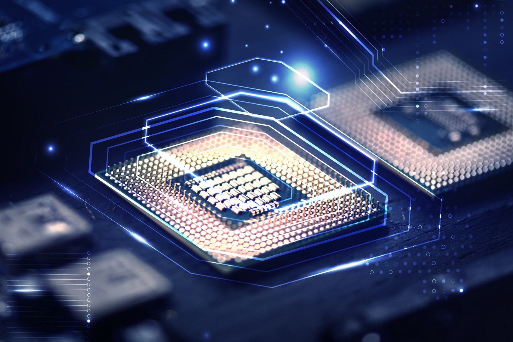
1. Precision: It is difficult to achieve adequate yield at emerging small geometries (current goal is 10nm – that’s one ten millionth of a millimeter while the diameter of an atom of silicon is not much smaller – 0.23nm) as is – electrical noise in the manufacturing equipment makes achieving required accuracy and yield quite challenging.
2. Process: Strong interference may alter the “recipe” of a process just enough to scrap expensive wafer and to start over lengthy process.
3. Equipment uptime (sometimes called “equipment availability”): If a tool is affected by electromagnetic interference to the degree where it can no longer guarantee required yield, that’s several millions of $$ standing idle while the wafers or packaged devices are not being processed.
4. Test: False positives or false negatives can either halt manufacturing process or cause faulty component to be shipped to a customer. Small geometry, high data speed and low-level signals make test equipment highly susceptible to unwanted electrical noise.
5. Device damage: Strong electromagnetic interference (EMI), specifically conducted emission with substantial energy, may be able to damage sensitive devices, especially in processes with metal-to-metal contact to the devices.
In addition, the other particular challenge facing semiconductor manufacturers is that the requirements of commonly-used EMC regulations and standards correspond poorly to the specific environment at the factory and to the key factors that actually affects equipment and process. Since EMC regulation compliance efforts are focused only on a single device, every "ingredient" in general may be satisfactory, but once all the equipment is up and running, the formed EMI graph may not look good. Especially in semiconductor fabs with diversified energy, fairly high EMI levels will be reached.
It is time to address and manage the ‘end goal’ in EMC compliance — EMI in actual applications: SEMI E176-1017 is the only document in the industry known to the author to provide practical guidance for that.
The guide is to provide guidance for the assessment and minimization of electromagnetic interference (EMI) in a semiconductor manufacturing environment to improve yield, equipment availability, and test results. This guide applies to equipment and facilities provided for the purpose of manufacturing semiconductor devices (i.e., equipment in a semiconductor manufacturing environment) not otherwise in the scope of SEMI E33, including all communications and control systems; processing, metrology, inspection, and automation equipment; and information-technology equipment. E176 is also unique because it is not limited just to semiconductor manufacturing, but has application across other industries. Back-end assembly and test, as well as PCB assembly are just as affected by EMI and can benefit from SEMI E176 implementation as there are strong similarities between handling of semiconductor devices in IC manufacturing and in PCB assemblies and prevention of defects is often shared between IC and PCB manufacturers.”
In the opening section, it outlines which specific properties of EMI are most harmful, some of which are not properly addressed in current EMC regulations, such as European EMC Directive, but are germane to manufacturing, among them peak amplitudes of signal, pulse width of a pulsed signal, ringing and alike. The section “Effects of EMI on Equipment, Semiconductor Devices, and Communication Systems” provides specifics on how excessive EMI negatively impacts equipment operation, data communication and, in some cases, sensitive semiconductor devices by causing electrical overstress (EOS). Electrical overstress is “the number 1 cause of damage to IC components” according to Intel. A detailed explanation is given on the impact of EMI on semiconductor devices, including direct damage from EOS and EMI-caused latch-up. For example, it outlines exposure to latch-up conditions of the devices caused by conducted EMI. High-level transients (i.e., high vs. the supply voltages and data signals amplitude) are quite capable of putting ICs into latch up, which causes excessive current through devices, overheating, and eventual catastrophic damage. EMI-caused voltages on the ground as low as 0.3 V are considered harmful to sensitive devices.
Dedicated to understanding the harsh environmental conditions faced by the semiconductor manufacturing industry in factories, our SS4/Ultra High Performance Series Single-Phase Power Line Filters have been applied by many manufacturers and assisted them in designing the best electromagnetic interference solutions.
Data sources: semanticscholar.org